
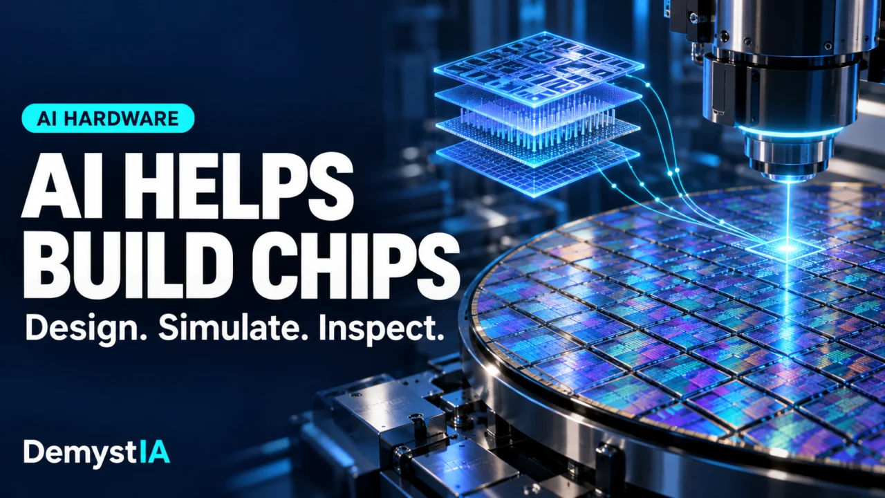
AI depends on advanced chips. Increasingly, the engineering tools used to develop those chips combine AI with faster simulation and data processing. The opportunity is to investigate more options before committing to expensive physical manufacturing.
On October 14, 2026, Nvidia announced expanded tools and collaborations for semiconductor design, simulation and inspection. Its announcement describes “AI-defined fabs,” where AI and accelerated computing assist engineering and factory operations.
The useful story is how those technologies fit together—and why a faster calculation should not be confused with a proportionally faster chip factory.
Why chipmaking needs so much computation
As ASML explains, microchips are built from interconnected patterns arranged in layers on a silicon wafer. Manufacturing involves hundreds of steps, with extremely precise alignment between layers.
Designing a circuit and manufacturing it are related but distinct activities. ASML distinguishes companies that design and manufacture chips, foundries that manufacture for customers, and fabless designers such as Nvidia that rely on manufacturing partners.
This helps clarify Nvidia’s announcement: supplying engineering software and computing infrastructure is different from operating the factory that physically makes a chip.
For an engineer, a proposed change creates several questions. Will the intended structure survive the manufacturing process? Will it behave as expected? Can it be produced consistently? Simulation offers a way to explore those questions before, and alongside, physical experiments.
AI, GPU acceleration and agents play different roles
These terms describe complementary capabilities. Treating them as interchangeable makes it harder to understand what an announcement actually demonstrates.
| Capability | What it contributes | What still needs checking |
|---|---|---|
| GPU-accelerated software | Runs supported calculations using GPU computing. | Whether the speed gain holds for the complete workload. |
| An AI model | Can estimate patterns or propose outputs based on its training. | Whether its output is accurate for the engineering case. |
| An AI agent | Coordinates steps and calls tools toward a defined goal. | Whether the sequence, tool settings and final result are appropriate. |
The distinction is visible in Nvidia’s own NPP documentation: NPP supplies CUDA-accelerated image and signal-processing functions. Calling such a function does not, by itself, demonstrate that a language model learned a better way to manufacture a chip.
Our explanation of Google’s Gemini agent explores the more general distinction between a model’s capabilities and the tools used to complete work.
Modeling materials before making changes
Nvidia’s new cuPotential library provides GPU-accelerated functions for simulations of atomic and molecular interactions. The company says developers can make these tools available to AI agents, with Synopsys among the early adopters.
An illustrative workflow would ask an agent to prepare a set of simulation runs, examine the results and identify candidates for further investigation. The simulation engine performs the calculations; the agent helps organize the work.
That separation matters. A plausible explanation written by an agent is not the same thing as a verified physical prediction. The useful output would include the simulation settings, assumptions and results needed for an engineer to inspect the conclusion.
Preparing patterns for lithography
One concrete example comes from Siemens’ separate October 14 announcement. The company is integrating Nvidia cuLitho into its Calibre manufacturing software to accelerate computational lithography.
This work concerns preparing patterns for manufacturing. Optical proximity correction, or OPC, adjusts mask patterns to account for how they will be transferred during lithography. Siemens says increasing pattern complexity makes these calculations a significant computational challenge.
The company reports up to 12 times faster full-chip OPC workloads. This is a Siemens performance claim for a defined type of work, not an independent DemystIA benchmark.
A shorter calculation could give engineers room to examine additional candidates or complete an iteration sooner. It does not establish that every subsequent manufacturing step becomes faster.
Testing a manufacturing process virtually
Lam Research’s SEMulator3D product description explains another part of the workflow. Its software combines design data with a description of manufacturing steps to build a virtual representation of the resulting three-dimensional structures.
Lam presents this as a way to understand manufacturing effects earlier and reduce the need for repeated physical learning cycles. The product page establishes what process modeling is intended to do; it should not be read as independent confirmation of every performance figure in a partner announcement.
Consider a hypothetical team changing a process setting. It could compare the predicted structures from several settings, reject unsuitable candidates and identify a smaller set for physical testing.
The value would come from narrowing the experiment intelligently. A convincing virtual model still needs an adequate connection to real measurements. Faster simulation is useful only if the modeled result remains relevant to the manufacturing problem.
Making inspection data easier to use
Nvidia’s announcement also describes KLA using NPP-based image processing and other partners applying accelerated analytics to semiconductor testing.
NPP’s documentation lists operations such as filtering, image comparison and geometric transformations. These are building blocks that developers can integrate into larger inspection applications.
For an illustrative inspection system, the steps might include preparing an image, comparing it with a reference and deciding which differences deserve investigation. The ability to process more images is one question; the ability to distinguish meaningful defects from harmless differences is another.
A useful assessment would therefore examine both processing time and detection quality. More rapid analysis has limited value if important defects are missed or engineers are overwhelmed by false alarms.
What the speed claims do—and do not—show
Nvidia reports a further 2–3 times acceleration for already GPU-optimized workflows in early-access cuPotential testing. The comparison starts from software that already uses GPUs.
That figure and Siemens’ OPC result measure different work. They should not be added together, multiplied into a factory-wide estimate or treated as a direct ranking of the products.
A simple hypothetical calculation shows why scope matters. Suppose a workflow takes ten hours: two hours of computation and eight hours of other work. Making the computation ten times faster reduces it to twelve minutes. The complete workflow still takes eight hours and twelve minutes—an eighteen percent reduction, rather than a tenfold improvement.
This example is an editorial calculation, not a measured semiconductor result. It illustrates why readers should ask which part of a process a benchmark measures and what remains outside it.
What is available now?
Nvidia lists cuPotential as early access, NanoVDB as open source within OpenVDB, and NPP as available through the CUDA Toolkit. The NanoVDB-accelerated SEMulator3D capability is targeted for release by the end of 2026.
These are different delivery stages. An available library is not evidence that every integration announced around it is already deployed in production.
What this could change for the chip industry
Our interpretation is that the opportunity lies in reducing the friction between proposing a change, testing it digitally and deciding what to validate physically.
For engineering teams, the benefit could take several forms: exploring more candidates within a fixed schedule, identifying problems earlier or reducing time spent moving information between specialized tools. Each outcome needs to be measured against the actual process.
For Nvidia, the announcement also highlights the importance of software around its hardware. Computing becomes more useful when it is integrated into the applications engineers already depend on.
AI is helping expand what can be explored in semiconductor engineering. The strongest evidence of progress will be validated improvements in useful work—not simply the largest speed multiplier in a press release.
Sources
- Nvidia — NVIDIA and Semiconductor Leaders Advance AI Across Chip Design and Manufacturing for AI-Defined Fabs, October 14, 2026. Announcement, cuPotential claims and availability.
- Siemens — Siemens transforms computational lithography for next-generation AI semiconductors with NVIDIA cuLitho, October 14, 2026.
- Lam Research — SEMulator3D, product description.
- Nvidia documentation — What is NPP?, library functions and role.
- ASML — How microchips are made, manufacturing background.
Sources checked October 15, 2026. Performance figures are vendor-reported, not results from independent DemystIA testing. Workflow examples and the time-saving calculation are illustrative.